


About the Cover
Vol. 82 No. 2 (2006)
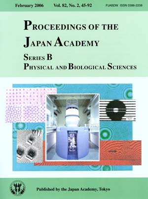
The Holography Electron Microscope was developed jointly by the Japan Science and Technology Agency (JST) and Hitachi, Ltd. and installed at Hatoyama, Saitama, Japan to explore the behaviors of quantum phenomena and objects in the microscopic world. The microscope is equipped with a coherent electron beam that is field-emitted from a pointed-tip cathode; this is the brightest beam ever obtained. This new technology opens new ways to directly observe hitherto-unobservable phenomena by utilizing the wave-nature of electrons.
Observation photographs using the phase information of electrons show vortices pinned by a regular array of artificial pinning centers in superconductors (upper left), thickness contours in fine MgO particles (lower left), evidence for the Aharonov-Bohm effect (upper right), and magnetic lines of force of the recorded pattern in a magnetic metal tape (lower right). The background photograph in green shows ripples of electron waves.